
Research Facilities
 |
 |
 |
 |
|
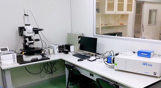
Raman System
A Raman spectroscope (Horiba) with three excitation sources fully integrated with AFM system.
|
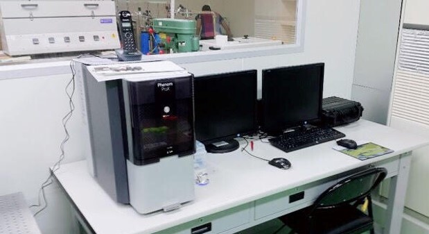
Scanning Electron Microscope (SEM)
A tabletop SEM (Phenom ProX) with BDS and EDS detectors.
|
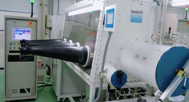
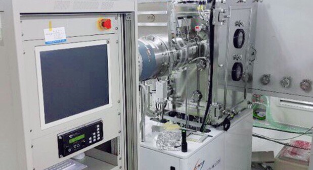
N2 Glove Box
A N2-filled glove box (MBraun) integrated with sputtering and thermal deposition systems.
|
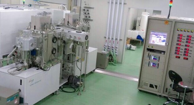
Large-area OLED Fabrication System
A custom-designed thermal evaporator (Syskey) for large-area organic electronic devices.
|
 |
 |
 |
 |
|
Photolithography system
A photolithography system with semi-auto aligner and exposure system (M&R Nano) for thin-film patterning.
|
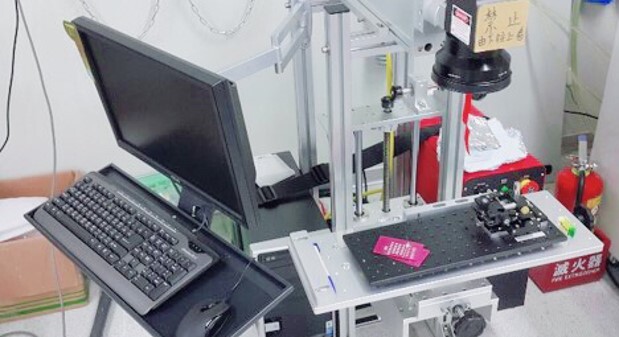
Laser etching system
Laser-direct-write dry etching with a 1064-nm laser for mask-free thin-film patterning.
|
Thermal Evaporator
A custom-designed system (Syskey) for simultaneous thermal deposition of organic materials and metals.
|
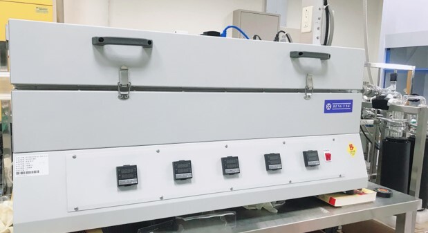
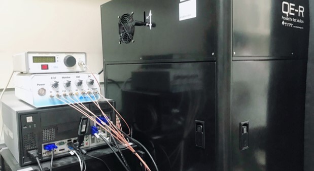
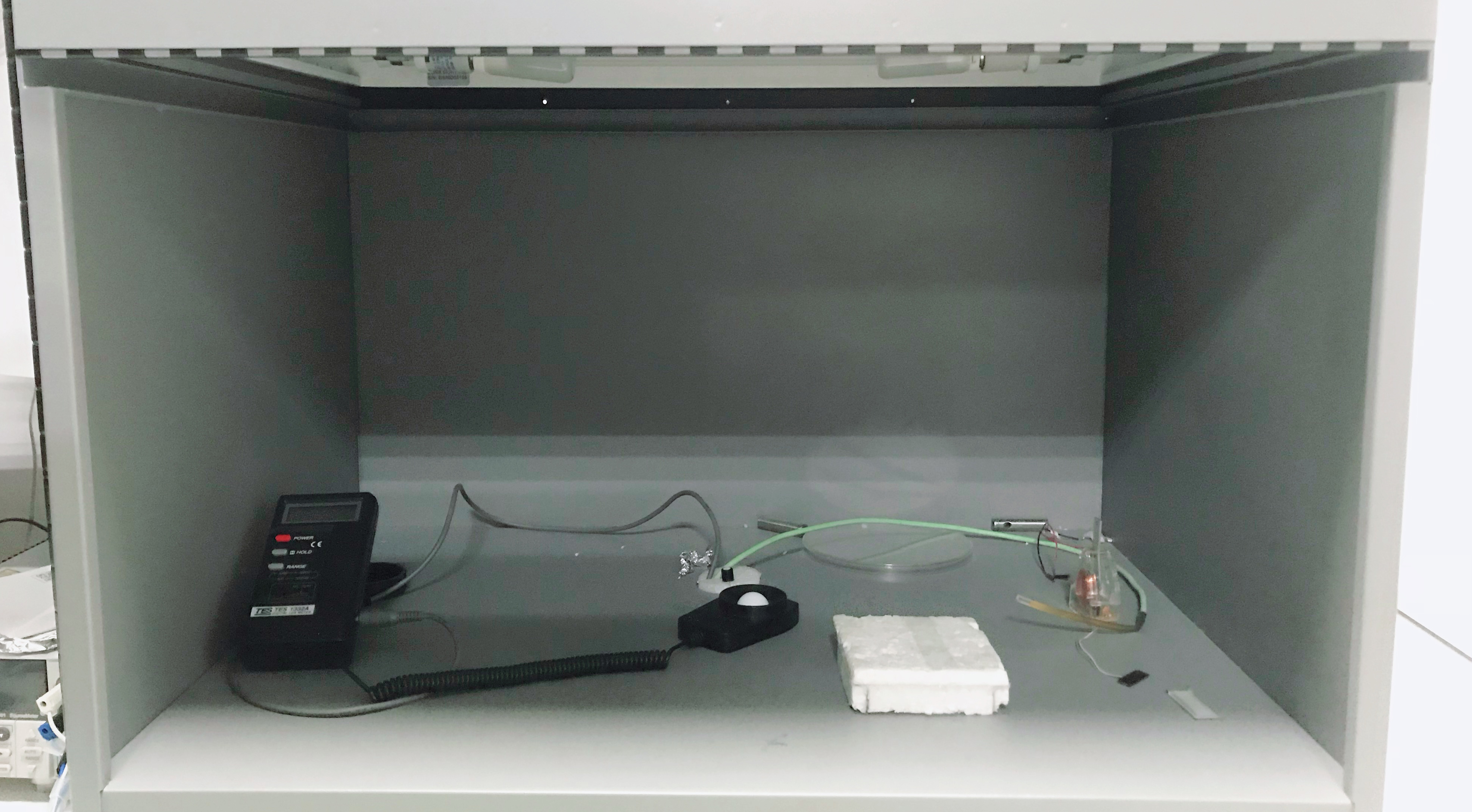
Photo-Response Platform
An electrical probe station (Everbeing Int'L) in multichannel black box for photo response measurements.
|
 |
 |
 |
 |
|
High-Vacuum Purification System
Graded sublimation for organic materials.
|
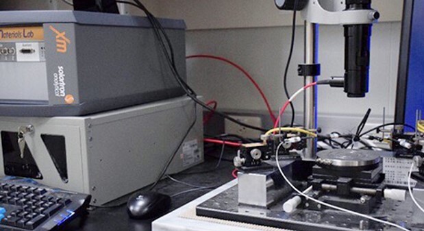
Impedance Measurement
An impedance measurement equipment (XM SOLARTRON analytical) is based on the frequency response analyzers for impedance/CV/RC.
|
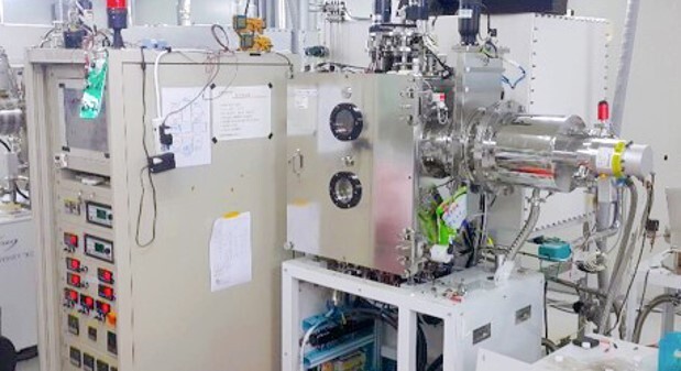
Sputter systet
A custom-designed sputter system with DC & RF Guns by Syskey Technology for dielectric material depositions.
|
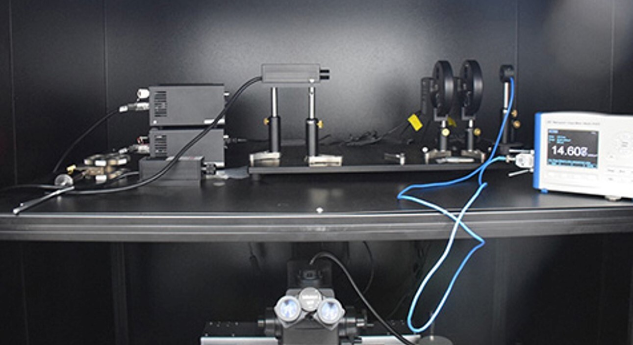
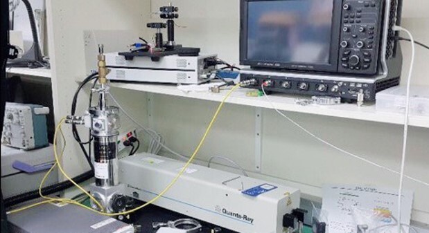
Time-of-Flight (TOF)
Time of flight (TOF) is an experimental technique used for the charge carrier mobility of organic semiconductors.
|
 |
 |
 |
 |
|
IPCE Measurement System
To evaluate the external quantum efficiency of solar cells.
|
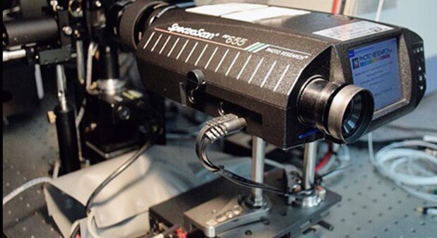
Electroluminescence Measurement
To obtain J-V-L characteristics and emission spectra of OLEDs using a PR-655 spectrophotometer.
|
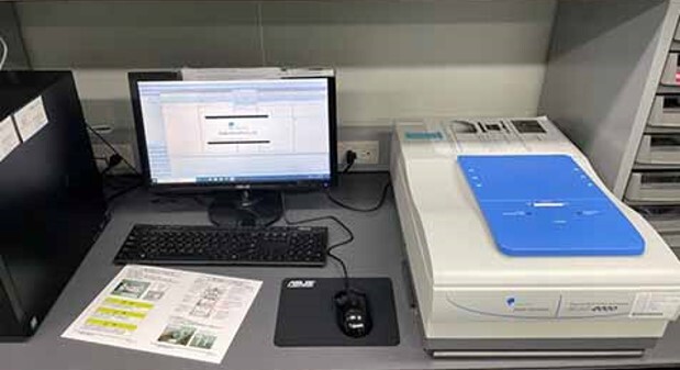
Ellipsometer
To obtain J-V-L characteristics and emission spectra of OLEDs using a PR-655 spectrophotometer.
|
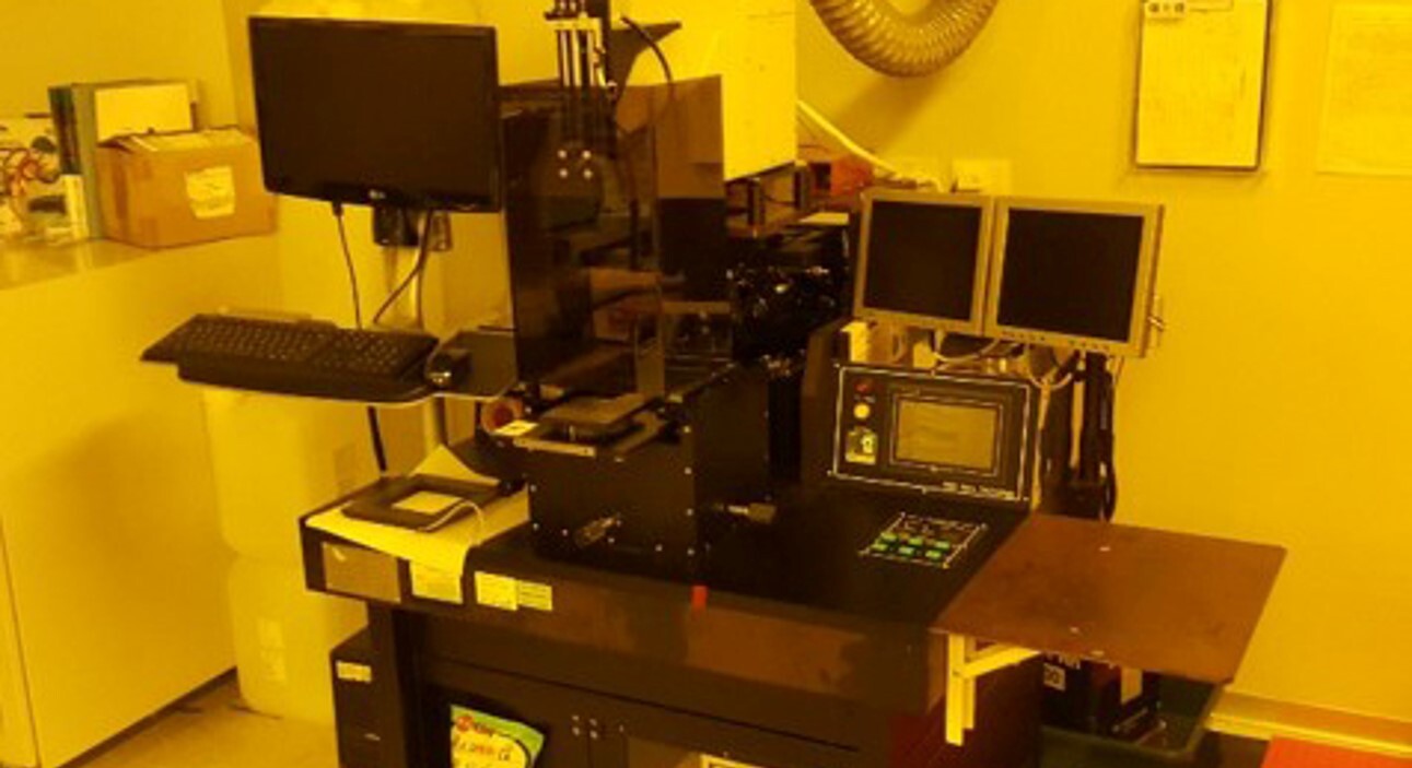
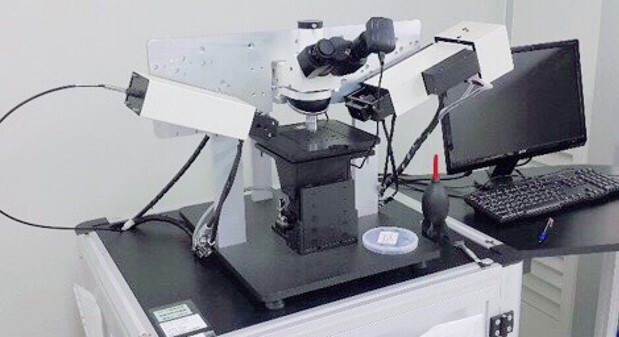
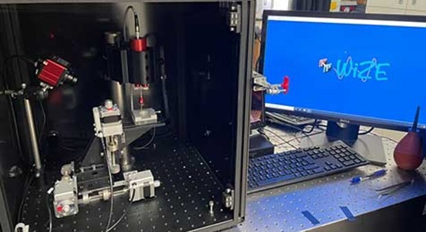
Atomic Force Microscope (AFM)
To obtain nano-scale surface topologic characterization with EFM and MFM functions.
|
 |
 |
 |
 |
|
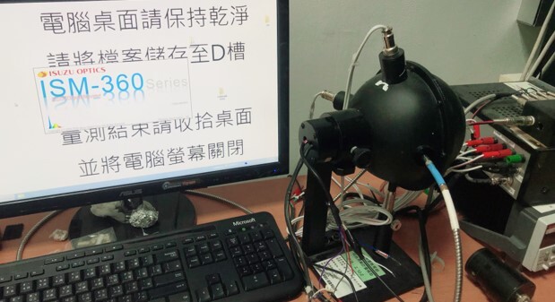
Electroluminescence Measurement
A photodiode system integrated with an integrated sphere is to evaluate the external quantum efficiency and power efficiency of OLEDs.
|
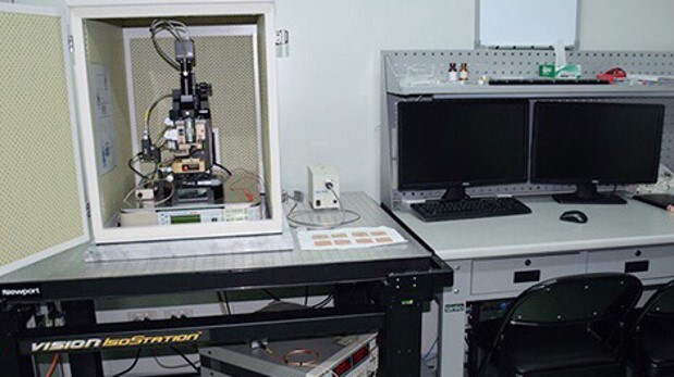
Semiconductor Characterization System
Keithley 4200 Parameter Analyzer has four SMU channels for organic semiconductor devices and each channel provides high resolution from 100fA to 0.1fA.
|
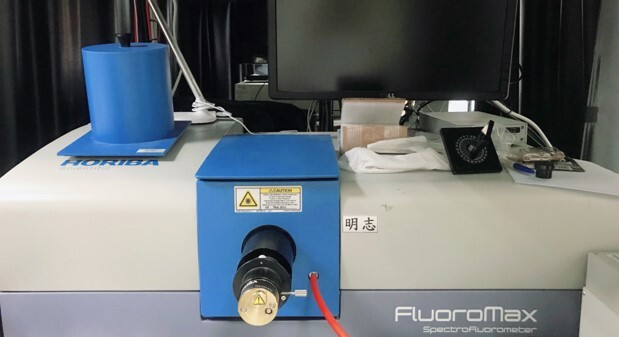
Time-Resolved Photoluminescence
A transient PL system (Horiba) with a Xe lamp as light source to provide a pico-second time resolution.
|
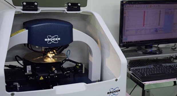
Surface Profile
The DektakXT stylus profilometer (Bruker) is a measurement of the peak-to-valley height of thin films with low noise and a 10-nm Z-axis resolution.
|
 |
 |
 |
 |
|
Indoor Solar Simulator
An indoor solar simulator from Industrial Technology Research Institute is to obtain energy conversion efficiency of photovoltaic devices under indoor lights.
|
Zeta Potentia
ELSZ-2000ZS (OTSUKA. Japan) can provide the colloidal particles' dispersion and aggregation, surface modification, and important surface zeta-potential et. al. by utilizing the dynamic electrophoretic light scattering method.
|
Kelvin Probe
KP5050 (KPTtech. UK.) uses contact potential difference to perform WORK FUNCTION of metal or organic/inorganic semiconductors in an atmospheric environment. This technology is expandable in the future for Fermi Level, Valence band and more.
|
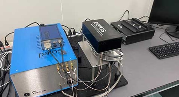
Paio
Paios can perform various electrical and optical characterizations on organic, perovskite and quantum-dot LEDs and solar cells, including the DC, AC and transient characteristics of OLED and solar cells, such as Photo-CELIV, Impednace, CV, TPV, TPC , TEL, DIT, CT, IMPS, IMVS and MELS. PAIOS can obtain consistent and accurate measurement data through simple measurement, and can directly fit all data to establish a reliable devices data database.
|